Journal of Applied Science and Engineering

Published by Tamkang University Press

1.30

Impact Factor

1.60

CiteScore

Kuei-Hsien Chen This email address is being protected from spambots. You need JavaScript enabled to view it.1,2, Chih-Hsun Hsu2 , Hung-Chun Lo1 , Surojit Chattopadhyay1 , Chien Ting Wu1 , Jih-Shang Hwang1 , Debajyoti Das1 and Li-Chyong Chen2

1Institute of Atomic and Molecular Science Academia Sinica Taipei, Taiwan 106, R.O.C.
2Center for Condensed Matter Sciences National Taiwan University Taipei, Taiwan 106, R.O.C


Received: March 21, 2004
Accepted: May 20, 2004
Publication Date: September 1, 2004

Download Citation: ||https://doi.org/10.6180/jase.2004.7.3.01  


ABSTRACT


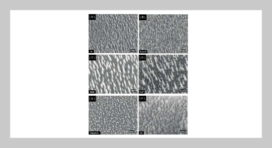
Well-aligned nanotip arrays were fabricated via a self-masking dry etching technique in an electron cyclotron resonance (ECR) plasma process. Nanotip arrays of Si, poly silicon, GaN, GaP, sapphire, and Al were fabricated. Simultaneous etching of the substrate and formation of silicon carbide (SiC) protecting caps are attributed to the nanotip formation. The ultra-low turn on filed for electron field emission as well as the surface enhanced Raman Spectroscopic study of Si nanotips is also demonstrated.


Keywords: Nanotip, Field Emission, Surface Enhanced Raman Spectroscopy.


REFERENCES


  1. [1] Ravi, T. S.; Marcus, R. B.; Liu, D. J. Vac. Sci. Technol. B 1991, 9, 2733.
  2. [2] Williams, C. C.; Davis, R. C.; Neuzil, P. US patent 5,969,345 (1999).
  3. [3] Nishijima, H.; Kamo, S.; Akita, S.; Nakayama, Y. Appl. Phys. Lett. 1999, 74, 4061.
  4. [4] Cho, K.; Joannopoulos, J. D. Phys. Rev. Lett. 1993, 71, 1387.
  5. [5] Striemer, C. C.; Fauchet, P. M. Appl. Phys. Lett. 2002, 81, 2980.
  6. [6] Ponce, F. A.; Bour, D. P. Nature 1997, 386, 351. Generally Applicable Self-masking Technique for Nanotips Array Fabrication 133
  7. [7] Lin, V. S. Y.; Motesharei, K.; Dancil, K. P. S.; Sailor, M. J.; Ghadiri, M. R. Science 1997, 278, 840.
  8. [8] Kovalev, D.; Timoshenko, V. Y.; Kunzner, N.; Gross, E.; Koch, F. Phys. Rev. Lett. 2001, 87, 68301.
  9. [9] Hickman, J. J.; Ofer, D.; Laibinis, P. E.; Whitesides, G. M.; Wrighton, M. S. Science 1991, 252, 688.
  10. [10] Hsu, C. H.; Lo, H. C.; Chen, C. F.; Wu, C. T.; Hwang, J. H.; Das, D.; Tsai, J.; Chen, L. C.; Chen, K. H. Nano Letters [Web published, 2004].
  11. [11] Lee, W. H.; Lin, J. C.; Lee, C.; Cheng, H. C.; Yew, T. R. Diam. & Relat. Mater. 2001, 10, 2075.
  12. [12] Yomaoka, Y.; Goto, T.; Nakao, M.; Kanemaru, S.; Itoh, J. Jpn. J. Appl. Phys. 1995, 34, 6932.
  13. [13] Lo, H. C.; Das, D.; Hwang, J. S.; Chen, K. H.; Hsu, C. H.; Chen, C. F.; Chen, L. C. Appl. Phys. Lett. 2003, 83, 1420.
  14. [14] Nie, S.; and Emory, S. R. Science 1997, 275, 1102.
  15. [15] Kneipp, K.; Yang, Y.; Kneipp, H.; Parleman, L. T.; Itzkan, I.; Dasari, R. R.; Feld, M. S. Phys. Rev. Lett. 1997, 78, 1667.
  16. [16] Xu, H.; Bjerneld, E. J.; Kall, M.; Borjesson, L. Phys. Rev. Lett. 1999, 83, 4357.
  17. [17] Fleishmann, M.; Hendra, P. J.; McQuillan, A. J. Chem. Phys. Lett. 1974, 26, 163.


1.6
2022CiteScore
 
 
60th percentile
Powered by  Scopus

SCImago Journal & Country Rank

Enter your name and email below to receive latest published articles in Journal of Applied Science and Engineering.