




B.E. Umirzakov, D.A. Tashmukhamedova, M.B. Yusupjanova, and B.O. Isakov
Tashkent State Technical University named after Islam Karimov, University Street, 2, Tashkent 100095, Uzbekistan
Received: February 6, 2026
Accepted: June 30, 2026
Publication Date: July 25, 2026
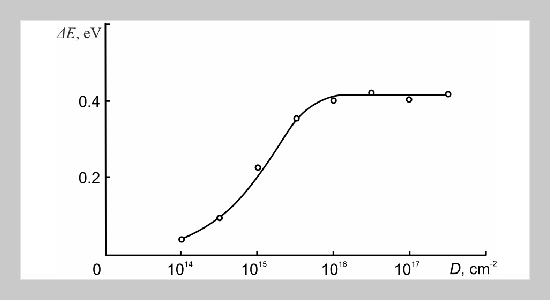
Dependence of the shift of peak A on the dose of Ar+ions for Si(111) bombarded with Ar+ ions at Eo = 1keV.
Copyright The Author(s). This is an open access article distributed under the terms of the Creative Commons Attribution License (CC BY 4.0), which permits unrestricted use, distribution, and reproduction in any medium, provided the original author and source are cited.
Download Citation: BibTeX | http://dx.doi.org/10.6180/jase.202610_33.050
The composition, crystalline, and electronic structure of the Si(111) surface bombarded with low-energy Ar+ and Ba+ ions at various doses were studied using scanning electron microscopy, Auger electron spectroscopy, and photoelectron spectroscopy. The following cases will be analyzed: 1) The influence of formation of various chemical bonds on the appearance of new peaks in the photoelectron spectrum. 2) Influence of crystal lattice
disorder on the energy positions of the principal spectral peaks of silicon and barium silicides. The analysis reveals that disordering of the Si(111) near-surface region causes a displacement of the main silicon peak by approximately 0.3–0.4 eV, whereas the formation of BaSi and BaSi2 phases induces a more pronounced shift in the range of 0.4-0.5 eV. A simple theory is developed that makes it possible to explain the results on the change in the density of state of the valence band electrons.
Keywords: electronic structure, ion bombardment, photoelectron spectroscopy, chemical bonds, crystal lattice, silicides, composition, dose, valence electrons, annealing
- [1] V. Vorobyov, A. Rogov, V. Nuzhdin, V. Valeev, and A. Stepanov, (2020) “Sputtering of silicon surface during low-energy high-dose implantation with silver ions” Technical Physics 65(7): 1156-1162. DOI: 10.1134/S1063784220070269.
- [2] T. Nemoto, S. Aonuki, R. Koitabashi, Y. Yamashita, M. Mesuda, K. Toko, and T. Suemasu, (2021) “Solar cell operation of sputter-deposited n-BaSi2/p-Si heterojunction diodes and characterization of defects by deep-level transient spectroscopy” Appl. Phys. Express 14: 051010. DOI: 10.35848/1882-0786/abfb87.
- [3] R. Gainutdinov, M. Khamadeev, E. Zajtseva, and M. Salakhov, (2012) “Photon density of states in optical nanomaterials and control of energy levels of atoms” Nanosystems: Physics, Chemistry, Mathematics 3(1): 56-63. URL: https://www.mathnet.ru/eng/nano659.
- [4] D. Gromov, O. Pyatilova, S. Bulyarosky, A. Belov, and A. Raskin, (2013) “Specific features of the formation of arrays of silver clusters from a thin film on a SiO2 surface” Physics of the Solid State 55(3): 619-623. DOI: 10.1134/S106378341303013X.
- [5] K. Hoppe, W. Fahrner, D. Fink, S. Dhamodoran, A. Petrov, A. Chandra, A. Saad, F. Faupel, V. Chakravadhanula, and K. Zaporotchenko, (2008) “An ion track based approach to nano- and micro-electronics” Nucl. Instr. Meth. B. 266: 1642-1646. DOI: 10.1016/j.nimb.2007.12.069.
- [6] D. Tashmukhamedova, M. Yusupjanova, A. Tashatov, and B. Umirzakov, (2018) “Study of the influence of implanted atoms on the coefficients of the sputtering of silicon and silicon with a thin oxide film” Journal of Surface Investigation 12(5): 902-905. DOI: 10.1134/S1027451018050117.
- [7] F. Priolo, T. Gregorkiewicz, M. Galli, and T. Krauss, (2014) “Silicon nanostructures for photonics and photovoltaics” Nature Nanotechnology 9: 19-32. DOI: 10.1038/nnano.2013.271.
- [8] K. Karabeshkin, P. Karaseov, and A. Titov, (2016) “Effect of an increase in the density of collision cascades on the efficiency of the generation of primary displacements during the ion bombardment of Si” Semiconductors 50(8): 989-995. DOI: 10.1134/S1063782616080145.
- [9] S. Donaev, B. Umirzakov, and D. Tashmukhamedova, (2015) “Electronic structure of Ga1–xAlxAs nanostructures grown on the GaAs surface by ion implantation” Technical Physics 60(10): 1563-1566. DOI: 10.1134/S1063784215100138.
- [10] R. L. Savio, L. Repetto, P. Guida, E. Angeli, G. Firpo, A. Volpe, V. Ierardi, and U. Valbusa, (2016) “Control of the micrometric scale morphology of silicon nanowires through ion irradiation-induced metal dewetting” Solid State Commun 240: 41-45. DOI: 10.1016/j.ssc.2016.04.023.
- [11] D. Tashmukhamedova, (2006) “Study of composition and electronic structure of CoSi2/Si interface” Bulletin of the Russian Academy of Sciences: Physics 70(8), 1409-1411. URL: https://elibrary.ru/item.asp?id=27854241.
- [12] E. Ergashov, D. Tashmukhamedova, F. Djurabekova, and B. Umirzakov, (2016) “Effect of surface microroughness on the composition and electronic properties of CdTe/Mo(111) films” Bulletin of the Russian Academy of Sciences: Physics 80(2): 138-140. DOI: 10.3103/S1062873816020064.
- [13] C.-M. Lee, S.-P. Chang, S.-J. Chang, and C.-I. Wu, (2013) “Fabrication of high-efficiency silicon solar cells by ion implant process” International Journal of Electrochemical Science 8(6): 7634–7645. DOI: 10.1016/S1452-3981(23)12832-X.
- [14] M. Eisa, J. Conradie, C. Mtshali, N. Mongwaketsi, and M. Maaza, (2026) “Optimization of ion beam elements using mathematical transport formalism” Journal of Applied Science and Engineering 30: 26030027. DOI: 10.6180/jase.202607_30.027.
- [15] M. Guzzo, G. Lani, F. Sottile, P. Romaniello, M. Gatti, J. Kas, J. Rehr, M. Silly, F. Sirotti, and L. Reining, (2011) “Valence electron photoemission spectrum of semiconductors: Ab Initio description of multiple satellites” Phys. Rev. Lett. 107: 166401. DOI: 10.1103/PhysRevLett.107.166401.
- [16] Z. Li, Y. Zhang, L. Ma, G. Tang, G. Wu, and F. Hu, (2022) “A new explanation on valence electron structure of C, Si, and Ge crystals with diamond structure based on photoelectron spectra” Journal of Electron Spectroscopy and Related Phenomena 254: 147153. DOI: 10.1016/j.elspec.2021.147153.
- [17] M. Yusupjanova, D. Tashmukhamedova, and B. Umirzakov, (2016) “Composition, morphology, and electronic structure of the nanophases created on the SiO2 Surface by Ar+ ion bombardment” Technical Physics 61, 628-630. DOI: 10.1134/S1063784216040253.
- [18] A. Keqi, M. Gehlmann, G. Conti, S. Nemšák, A. Rattanachata, J. Minár, L. Plucinski, J. Rault, J. Rueff, M. Scarpulla, M. Hategan, G. Pálsson, C. Conlon, D. Eiteneer, A. Saw, A. Gray, K. Kobayashi, S. Ueda, O. Dubon, C. Schneider, and C. Fadley, (2018) “Electronic structure of the dilute magnetic semiconductor Ga1–xMnxP from hard x-ray photoelectron spectroscopy and angle-resolved photoemission” Physical Review B. 97(1523): 155149. DOI: 10.1103/PhysRevB.97.155149.
- [19] F. Gygi, (2023) “All-Electron Plane-Wave Electronic Structure Calculations” Journal of Chemical Theory and Computation 19(4): 1300-1309. DOI: 10.1021/acs.jctc.2c01191.
- [20] N. Zikrillaev, K. Iliev, G. Kushiev, S. Isamov, S. Koveshnikov, B. Abdurakhmanov, and B. Isakov, (2026) “Study of photocells based on GexSi1–x structures” Journal of Applied Science and Engineering 29(03): 685-691. DOI: 10.6180/jase.202603_29(3).0019.
- [21] B. Umirzakov, D. Tashmukhamedova, and F. Khudaykulov, (2022) “Effect of implantation of Ba+ ions on the composition, electronic and crystal structure of W(111) and WO2 surfaces” Journal of Surface Investigation 16(6): 992-996. DOI: 10.1134/S1027451022050202.
- [22] A. Kazansky and K. Khabarova, (2004) “Distribution of the density of electronic states in the energy gap of microcrystalline hydrogenated silicon” Semiconductors 38(10): 1221-1224. DOI: 10.1134/1.1808833.
- [23] T. Zhdanova, V. Ilyasov, and I. Nikiforov, (2001) “Specific features of the electronic band structure and X-ray spectra of boron nitride in sphalerite and wurtzite modifications” Physics of the Solid State 43(8): 1445-1448. DOI: 10.1134/1.1395081.
- [24] O. Yastrubchak, N. Tataryn, L. Gluba, S. Mamykin, J. Sadowski, T. Andrearczyk, J. Domagala, O. Kondratenko, V. Romanyuk, O. Fedchenko, Y. Lytvynenko, O. Tkach, D. Vasilyev, S. Babenkov, K. Medjanik, K. Gas, M. Sawicki, T. Wosinski, G. Schönhense, and H.-J. Elmers, (2023) “Influence of Bi doping on the electronic structure of (Ga,Mn)As epitaxial layers” Sci Rep. 13: 17278. DOI: 10.1038/s41598-023-43702-w.
- [25] M. Sumiya, S. Ueda, K. Fukuda, Y. Asai, Y. Cho, L. Sang, A. Uedono, T. Sekiguchi, T. Onuma, and T. Honda, (2018) “Valence band edge tail states and band gap defect levels of GaN bulk and InxGa1–xN films detected by hard X-ray photoemission and photothermal deflection spectroscopy” Appl. Phys. Express 11: 021002. DOI: 10.7567/APEX.11.021002.
- [26] Y. Zhuravlev and A. Poplavnoy, (2003) “The distribution of the valence electron density in predominantly ionic crystals with different Bravais sublattices” Physics of the Solid State 45(1): 36-40. DOI: 10.1134/1.1537406.
- [27] V. Mikushkin, (2018) “Quantum well on the n-GaAs surface irradiated by argon ions” JETP Letters 107(4): 243-246. DOI: 10.1134/S0021364018040094.
- [28] V. Yarzhemsky, S. Murashov, and A. Izotov, (2019) “Electronic structure and ferromagnetic transition temperature of Ga1–xMnxAs in the nonempirical local exchange method” Inorganic Materials 55: 1-8. DOI: 10.1134/S0020168519010187.
- [29] M. Karimov, U. Kutliev, S. Bobojonova, and K. Otabaeva, (2021) “Investigation of angular spectrum of scattered inert gas ions from the InGaP (001) surface” Physics and Chemistry of Solid State 22(4): 742-745. DOI: 10.15330/pcss.22.4.742-745.
- [30] U. Kutliev, M. Otabaev, M. Karimov, F. Masharipov, and I. Woiciechowski, (2023) “Scattering of low-energy Ne+ ions from the stepped surface of InGaP(001)<110> at the small angles of incidence” Physics and Chemistry of Solid State 24(3): 542-548. DOI: 10.15330/pcss.24.3.542-548.
- [31] B. Umirzakov and S. Donaev, (2017) “On the creation of ordered nuclei by ion bombardment for obtaining nanoscale Si structures on the surface of CaF2 films” Journal of Surface Investigation 11: 746-748. DOI: 10.1134/S1027451017040139.
- [32] B. Umirzakov, D. Tashmukhamedova, M. Ruzibaeva, F. Djurabekova, and S. Danaev, (2014) “Investigation of change of the composition and structure of the CaF2/Si films surface at the low-energy bombardment” Nuclear Instruments and Methods in Physics Research Section B: Beam Interactions with Materials and Atoms 326: 322-325. DOI: 10.1016/j.nimb.2013.10.094.
- [33] S. Abraeva, D. Tashmukhamedova, S. Gulyamova, M. Yusupjanova, and A. Xujaniyazova, (2023) “Impact of bombardment by Ar+, Na+ and O2+ ions on spectra of elastically scattered electrons of single-crystal Ge” E3S Web of Conferences 401: 05006. DOI: 10.1051/e3sconf/202340105006.
- [34] D. Tashmukhamedova and M. Yusupjanova, (2021) “Formation of nanoscale structures on the surface of MgO films upon bombardment with low-energy ions” Journal of Surface Investigation 15(5): 1054-1057. DOI: 10.1134/S1027451021050402.
- [35] D. Tashmukhamedova, B. Umirzakov, and M. Mirzhalilova, (2004) “Structure and properties of nanocrystals grown in near-surface ranges of Si and GaAs by low-energy ion implantation” Izvestiya Akademii Nauk. Ser. Fizicheskaya 68(3): 424-427. (in Russian): URL: https://www.elibrary.ru/item.asp?id=17641066.
- [36] K. Boltaev, D. Tashmukhamedova, and B. Umirzakov, (2014) “Structure and electronic properties of nanoscale phases and nanofilms of metal silicides produced by ion implantation in combination with annealing” Journal of Surface Investigation 8(2): 326-331. DOI: 10.1134/S1027451014010108.
- [37] K. S. Thorne and R. D. Blandford. Statistical Physics: Volume 1 of Modern Classical Physics. Princeton University Press, 2021. URL: https://press.princeton.edu/books/paperback/9780691206127/statistical-physics.
- [38] K. W. Böer and U. W. Pohl. Semiconductor physics. Springer Nature, 2023. URL: https://link.springer.com/referencework/10.1007/978-3-031-18286-0.
- [39] F. Kugler, (2018) “Counting Feynman diagrams via many-body relations” Phys. Rev. E. 98: 023303. DOI: 10.1103/PhysRevE.98.023303.
- [40] R. M. Martin. Electronic structure: basic theory and practical methods. Cambridge University Press, 2020. DOI: 10.1017/9781108555586.